Asynchronous Counter Design
Problem Statement
Using what you learned from the SSI(small Scale) asynchronous counters, design a 3-bit counter(using D Flip-Flops) that counts from 0-5 in Multisim. Then modify this circuit and make it, start at 2 and end at six. After you have done that bread board your two designs on your bread board using the bread board companion as a clock. Last transfer the multisim designs into the DLB and prove that it works.
Constraints
-Create the circuits using Multisim
-Use D flip Flops
-Breadboard Circuit
-Program circuit into DLB
-Use D flip Flops
-Breadboard Circuit
-Program circuit into DLB
Calculations
We will be creating 3-Bit Mod Counters just like in the last assignment. I can see that these circuits will be more complicated though. They are plementing NAND gates into the circuit so this will probably have a profound effect on the count. I think that by changing the wires on the NAND gate we will be able io make the (2-6) counter. Also their is a SSD instead of a Hex Display and their is a encoder before it.The reason for that is that Hex displays are just digital and not real so we will have to bread board it.
Documentation
3-Bit Mod 6 Up Counter(0-5)
So we are given the first counter. All I had to do was wire it up in Multisim.The way the circuit works is pretty simple,as you can see in the video above the NAND gate gets three inputs from the three flip flops. If all the NAND's inputs came from Q the counter would count to 6 cause the NAND gate would allow all of the binary Qs to reach 1 and 111 in binary is 6, but this is not the case. the first flip flop's Q' is wired to the NAND gate. When Q1 and Q2 reach 1,Q0 will stay at zero cause clear will be at 0 and preset at one, which will make Q 0 and then every thing will reset back to 0. This means that the counters maximum binary count will be 110 which is 5 in the SSD.
3-Bit Mod 7 Up Counter(2-6)
To modify the 0-5 circuit we had to do a little bit of changes. First we changed one of the NANDS inputs from Q' to Q from the first flip flop. This meant that 3 bit will reach its maximum count as a explained above, when Q 0,1,2 all get 1s.Q0 will give you 1 cause 2^0 is 1 Q1 will give you 2 cause 2^1 is 2,and Q2 will give us 4 cause 2^2 is 4.If we add this up it will give us a binary count of 7 which is what we want in order for the counter to count to 6.So the counter clocks from 0 to 6 now but we had to make it reset/start at 2.To do this we had to wire the middle flip flop's clear to VCC and preset to the NAND gates output. Since clear is always one 1, the middle flip flops pulse will be based on weather preset is 1 or 0.preset is wired to the NAND gate so when all the flip flops go back to 0 and reset ,the middle flip flop will keep its 1 cause both preset and clear are at 1. Q1 will give us 2 cause 2^1 is 2 and this causes the clock to reset at 2.
3-Bit Mod 6 Up Counter(0-5) PLD
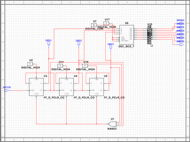
This was pretty much the easy work. I just had to remake my circuits in a PLD version to program them into the DLB. The only changes were the connectors. As you can see their was no SSD cause we actually have to have that on the DLB. It was replaced by each one of the segments in the SSD which would tell the SSD what number to display and inverters(74LS04) had to be placed in order to make the SSD work. All of the VCCs and GND are replaced by the digital highs and lows which are basically the same thing.Their is also a clock on the DLB so we replace that with a GPIO so we could manually wire the GPIO to the clock on the DLB and it would wok the same as on Multisim.
3-Bit Mod 7 Up Counter(2-6) PLD
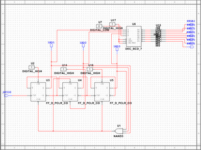
So this is the same circuit as the original one I made on Multisim. Did the same changes, changed clear to VCC which is represented by digital high and changed preset to get its input from the NAND gate. Also changed one of the NANDs input to Q as I did on my original 3-Bit mod counter, everything else stayed the same.
Final Design
3-Bit Mod 6 Up Counter 0-5(Breadboard)
Basic stuff, just had to implement new chips according to my design. The first two chips are the 74LS74N(D flip flops). Each chip contains two D flip flops and we only use three. The chip below that, is a three input NAND gate(74LS10N).The LEDs are on the bread board companion so I had to get inputs from each one of the chips. After that chip is the encoder(74LS47) this chip turns the binary inputs into info for the SSD to display. The two chips in the bottom that are next to each other are the inverters(74LS04). After I wired that the wires had to go through (220 ohm) resistors or else the SSD might not work. The clock is on the bread board companion and as you can see on the video I speed up the count.
3-Bit Mod 7 Up Counter 2-6(Breadboard)
Just had to change the wires around like I did on my Multisim design. Kind of hard to the right pace to put the wires but I got it done. My battery kinda sucks so the numbers kind of fade at the end of the video. you can find the schematics for each one of the chips that I used at www.alldatasheets.com
3-Bit Mod 6 Up counter(0-5)DLB
This is my 3-Bit Mod 6 Up counter on the Digital Logic board. I transferred my Multisim design into the logic board and as you can see there is a wire going from GPIO-0 to Rot CLK the reason is because in the PLD design their are no digital clocks so I have to use the one on the DLB. Since the clock is a negative edge triggered clock we must set the knob on the DLB to Low as seen on the video.
3-Bit Mod 7 Up counter(2-6)
This is the 3-Bit Mod 7 Up Counter that I programed into the DLB. Their was really not much work to do. I rewired my PLD accordingly to my 3-Bit Mod 7(2-6)that I had created and reprogramed the DLB.
Reflection
This project really made me notice how the binary counting is applied into circuits. each one of the flip flops makes the count get bigger. What was most surprising to me is how we can control the count limit and the count start by simply implementing NAND gates. At the start of this assignment I was kind of lost I couldn't figure out how to make the counter start at 2.It was pretty easy to make it count to 6 but I couldn't figure how to make it start at two. With the help of Mr. Wemp I figured out how to make the counter start at 2 and really began to understand how NAND gates work with the flip flops and how we can interrupt a clocks pulse by simply switching around wires from the flip flops and adding NAND gates. I think that we can implement different types of gates to have the same effect or even change the #s between the count.
Another thing that I was reminded of,was of the advantages of the DLB. When I heard that we had to bread board it I new that it would be a pain in the butt. I am more accustomed to the bread board now but it still took kind of long and the disadvantages of manually bread boarding came up again. I had to look up each one of the schematics for each one of the chips keep on looking back and fourth so I wouldn't mess up. Also one of my wires that powered a row was broken and I couldn't see it I had to go back and change my wires around and I couldn't find the problem until I touched the wire and finally swapped it with a good one. With the DLB I had none of that all I had to do was program the PLD which contained a digital circuit into the digital logic board and connect a GPI0 into the clock and I was done. To manually bread board I took about an hour maybe more, but it only took me about 5 minutes to program and have the DLB counting. The DLB is such a time saver and there is no mistakes you can make if you make the PLD according to the original the original design ,this is why it is way better than bread boarding manually. I hope that we can finally move on from manually bread boarding and just have our circuits be digitalized.
Another thing that I was reminded of,was of the advantages of the DLB. When I heard that we had to bread board it I new that it would be a pain in the butt. I am more accustomed to the bread board now but it still took kind of long and the disadvantages of manually bread boarding came up again. I had to look up each one of the schematics for each one of the chips keep on looking back and fourth so I wouldn't mess up. Also one of my wires that powered a row was broken and I couldn't see it I had to go back and change my wires around and I couldn't find the problem until I touched the wire and finally swapped it with a good one. With the DLB I had none of that all I had to do was program the PLD which contained a digital circuit into the digital logic board and connect a GPI0 into the clock and I was done. To manually bread board I took about an hour maybe more, but it only took me about 5 minutes to program and have the DLB counting. The DLB is such a time saver and there is no mistakes you can make if you make the PLD according to the original the original design ,this is why it is way better than bread boarding manually. I hope that we can finally move on from manually bread boarding and just have our circuits be digitalized.
