Flip Flop Applications
As the title of this portfolio entry states, we learned how flip flops are applied into real life circuits. The first circuit we built was a photo sensitive event detector and it works pretty simple. Then we built a 4 bit shift register detector and this was a bit more complex cause it contained four clocks(hence the name 4 bit shift) we had to enter certain input pulse from either ground or vcc in order to change the held input cause the clocks were wired in an event detect format as shown below.
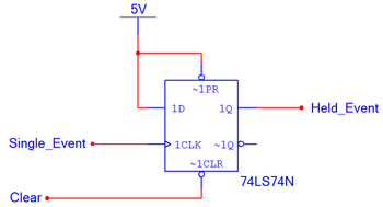
Event Detect Circuit
This is a D flip flop in a event detector format that I used to wire the photosensitive and the 4bit shift register circuits. The way it works is that when pulse(event) goes in, Q holds the pulse until another event(in this case clear) changes and their for changes the Q back to 0.
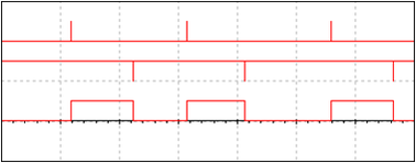
Below there is a timing chart that shows how the event detector works. The clock pulse(single event) tells Q pulse(held event) to switch to 1 and it is held by Q until clear pulses and turns Q to 0.
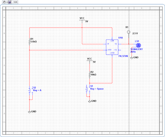
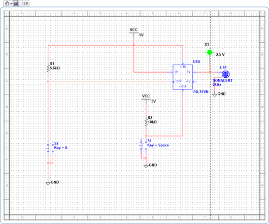
Photosensitive Event Detector
This is the photosensitive event circuit. This circuit would be used as a larger house burglar system. The SONALERT would sound the alarm if the beam of light between the 12-vlot bulb and the phototransistor(In this case the key A) is disrupted. When we cut GND off the clock gets a pulse of 1 and it checks preset and clear and since both clear and preset are wired to VCC 1 it is allowed to check D, which is also 1 so it tells Q to turn to 1 and this causes the SONALERT to sound the alarm. Although Key A goes back to GND the circuit is formatted in a event detect way so Q holds the pulse. To turn off the alarm Key B must be pressed so clear can turn to 0.When clear is one, the clock will check clear and preset and as I told you in my Intro to Flip Flops entry when preset is 1 and clear is 0 Q will default to 0 and this in turn will switch the alarm off.
Simulation
This is how the circuit simulation began I put a probe to show you when 1(power) would pass since you cant hear the alarm. So in the picture below I haven't touched nothing and A is wired to GND so it doesn't let the clock pulse. As you can see there is no power going to the SONALERT so the probe doesn't turn on.
When I pressed key A it cut off GND the clock started pulsing it checked D and made Q 1.This made the probe turn on which represents the alarm sounding. To turn the alarm off I just press Key B. It makes clear 0 which the clock checks and makes Q 0 and this makes the probe turn off.
4-Bit Shift Register
Basically a shift register is a group of flip flops(typically 4 or 8) that are arranged in an event detect format and pass the values from one flip flop to another. Shift register are usually used in logic circuits to control digital displays A real world example of shit registers being used is like when you type a number into the calculator and they shift to the left.
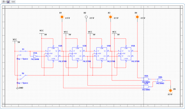
JK 4-Bit Register
The design below is a JK 4-Bit Register. It contains 4 negative edge triggered JK flip flops(74LS76N) so they must be wired to GND in order to pulse. The 4 probes on top show what output is coming out of Q and there are two SPDT switches connected to VCC and GND. So the way this 4 bit register works is that it moves the held input data that Q holds to the next every time the clock pulses. Since both our asynchronous inputs(preset and clear) are wired to VCC we don't care about them cause they will always let the clock pass so we must treat this like a normal JK flip fop. When the first SPDT is toggled it flips the J and K input from 1,0 or 0,1 cause of the inverter that we put.This gives the clock an out put of 1 when the SPDT switch is connected to VCC and 0 when it is connected to GND.IN order for the clock to pulse it must be connected to GND(0) cause it is a negative edge triggered clock. So by turning the SPDT of either the clock or the JK inputs to either VCC or GND we can light or turn of the first probe and shift it over to the next.There are 2 AND gates that are wired to either Q or Q' and these AND gates are connected to another AND and this AND is connected to a probe. As the problem stated I had to produce a certain binary combination(1101) which reads form left to right. Once I achieved this I had to make the bottom probe light up. To do this I simply connected to the outputs that give me one the probe that isn't lighting up is cause it is getting an input of 0 from Q,Q' is the opposite so I wired the NAND gate to that to get 1. When the probe gets all 1s it lights up as shown on the snippet below.
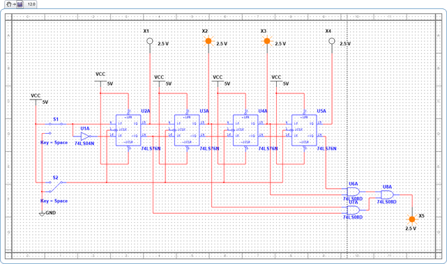
The snippet below just shows a different combination of clock pulses and JK toggling which gave us the binary combination of 0110.To make the bottom probe read this I wired the NAND gates to the two Qs in the middle that outputted a 1 and the two outer Q' that also outputted 1s.
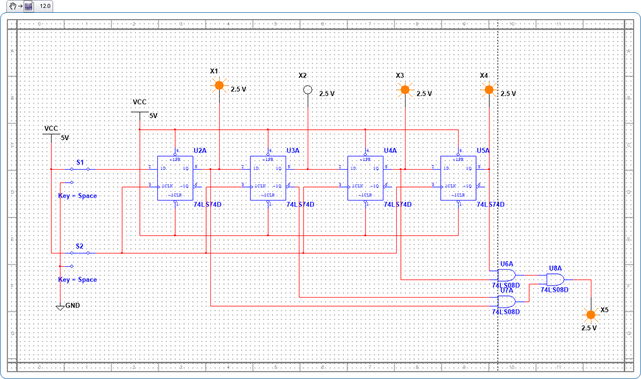
D 4-Bit Register
The 4-Bit shift register of the bottom is equivalent to the previous one I made except it is made completely out of D flip flops(74LS74D).It works exactly the same way and is basically wired the same. Our asynchronous inputs are wired to VCC so they don't interfere, and in order for the binary combination to light up we must wire the probes the same way I did on the top. The only difference is that we can get rid of the inverter and just work with D or D' so the light either turns on or off and the clock shifts the info on to the next. below I replicated the binary combination of 1101 that was first requested to make for the JK register. The only advantage I see on using the D flip flop is that we loose the inverter hence making the circuit more simple to read and more straight forward.